BTAudio Testbed Setup
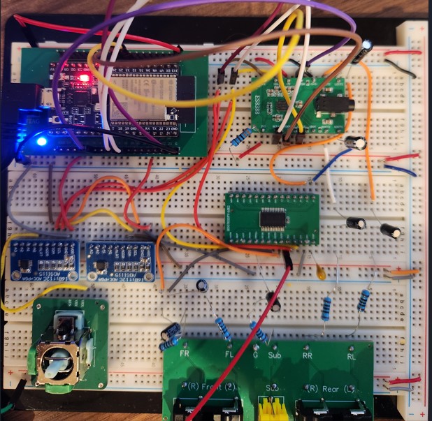
Below is the current setup for the BTAudio breadboard testbed. There are a lot of wires and a bunch of passives so I recommend doing this in stages and testing each stage before proceeding to the next.
Component Placement
I recommend spacing the components out as described below to support moving wires around as we test various things.
- Place the esp32 breadboard adapter and the codec on one row with a few spaces between them. The breadboard adapter should have the USB port facing left and the codec should have the headphone jack facing right. Position the codec so that there are two holes available on the bottom pins.
- On the second breadboard (below top one) place the two ADS115 breakouts on the left and the BD37033 breakout board on the right.
- Position ADS115’s with pins facing up, toward the ESP32 above it
- Position the BD37033 with the lable on the left, so MIN -> A1 are facing up towards the codec
- On the third breadboard place the RCA breakout board on the right. You can add any pots or other things on the left or below that (if you have a 4-breadboard setup)
- We’ll get power from the USB and run everything (except the BD37033, more on that later) off 3.3v. So, connect a F/M jumper from 3V3 and GND on the ESP32 to a a PWR/GND rail then connect all of the PWR/GND rails together.
Wiring
ESP32 to Codec
First connect the ESP32 and the codec. Once this is complete you should be able to load firmware and test bluetooth output to the headphone jack on the codec breakout. The LED will show blue when Bluetooth is ready and green once you connect. Once connected you should be able to stream audio from any source on your device.
I2S
I2S is used for streaming audio from the esp32 and is only used by the codec, therefore it can be connected directly
- Connect a F/M jumper from GPIO 0 on the ESP32 to MCLK on the codec
- Connect a F/M jumper from GPIO 5 on the ESP32 to BCLK on the codec
- Connect a F/M jumper from GPIO 25 on the ESP32 to LRCLK on the codec
- Connect a F/M jumper from GPIO 26 on the ESP32 to SDOUT on the codec
- Connect a F/M jumper from GPIO 19 on the ESP32 to SDIN on the codec
I2C
I2C is used by several components so we don’t want to connect directly to the codec. Instead we’ll utilize a few of space breadboard spaces between the esp32 and the codec and jumper from there
- Connect a F/M jumper from GPIO 23 on the ESP32 to a middle column, then a M/M jumper from there to SCL on the codec
- Connect a F/M jumper from GPIO 18 on the ESP32 to a middle column, then a M/M jumper from there to SDA on the codec
Others
- Connect 3V3 on the codec to a shared 3.3v power rail
- Connect GND on the codec to a shared GND power rail
- Connect CE on the codec to a shared GND power rail
- Place a 3.3kΩ resistor from 3V3 on the codec to a shared GND power rail. Note: This just provides a poweroff discharge path and isn’t strictly required, but I recommend adding it so that you mimic my setup.
ADS1115 (x2)
For our initial testing we’ll use 3.3v. We’ll need to figure out how to handle 5v signals but we can do that once everything else is setup and working.
- Connect VDD/GND pins on both boards to shared PWR/GND
- Connect SCL and SDA on both board to the shared I2C columns you made earlier. Alternatively you can connect one set then connect the second board to those pins on the first, either will work
- On the left ADS1115, connect the ADDR pin to shared GND
- On the right ADS1115, connect the ADDR pin to shared PWR
BD37033 & RCA breakout board
Here we’ll wire the ES83033 codec to the BD37033 audio processor then out the RCA jacks.
Here is the wiring from the ES8388 to the BD37033. Only two pins are currently used on the top row of the BD37033
- Connect a 1uF capacitor from the LOUT1 pin on the ES8388, with (-) side facing the ES8388, to an open breadboard column. Then add a jumper from there to A2 pin on the BD37033
- Connect a 1uF capacitor from the ROUT1 pin on the ES8388, with (-) side facing the ES8388, to an open breadboard column. Then add a jumper from there to A1 pin on the BD37033
Here is the rest of the wiring for the BD37033. These are all on the bottom row (facing the RCA breakout board) and listed from left to right.
- Connect a 10kΩ resistor from the MUTE pin to any shared 3V3 rail
- Connect a 10kΩ resistor from the LRST pin to any shared 3V3 rail
- Connect a 100nF (0.1uF) capacitor from the LOUT pin to any shared GND rail
- Connect the OUTS1 pin to the Sub RCA pin through a 10uF capacitor and 100Ω resistor
- (+) side of capacitor faces the OUTS1 pin
- Order is: OUTS1 -> 10uF -> 100Ω -> Sub
- resistor can be omitted if space is tight
- Connect the OUTR2 pin to the RL RCA pin through a 10uF capacitor and 100Ω resistor
- (+) side of capacitor faces the OUTR2 pin
- Order is: OUTR2 -> 10uF -> 100Ω -> RL
- resistor can be omitted if space is tight
- Connect the OUTR1 pin to the RR RCA pin through a 10uF capacitor and 100Ω resistor
- (+) side of capacitor faces the OUTR1 pin
- Order is: OUTR1 -> 10uF -> 100Ω -> RR
- resistor can be omitted if space is tight
- Connect the OUTF2 pin to the FL RCA pin through a 10uF capacitor and 100Ω resistor
- (+) side of capacitor faces the OUTF2 pin
- Order is: OUTF2 -> 10uF -> 100Ω -> FL
- resistor can be omitted if space is tight
- Connect the OUTF1 pin to the FR RCA pin through a 10uF capacitor and 100Ω resistor
- (+) side of capacitor faces the OUTF1 pin
- Order is: OUTF1 -> 10uF -> 100Ω -> FR
- resistor can be omitted if space is tight
- Connect the VCC pin to any shared GND via a 10uF capacitor
- Connect the VCC pin to bench power via a jumper wire (and bench gnd to any shared GND rail).
- Note that voltage range is 7v to 9.5v but I recommend setting to 8.5v since that’s likely what the final board will use. The chip only uses about 20mA of current so you might get away with a 9v battery/barrel jack if bench power isn’t easily available, though I haven’t tried this.
- Connect the SCL pin to the shared I2C SCL row you made earlier
- Connect the SDA pin to the shared I2C SDA row you made earlier
- Connect the GND pin to any shared GND rail
- Connect the VREF pin to any shared GND using a 10uF capacitor
- Connect the G pin on the RCA breakout baard to any shared GND rail
At this point you should be wired in and ready to test. Since the BD37033 uses a higher voltage than the rest of the testbed it’ll need to be fed between 7v and 9.5v separately, though i’d recommend 8.5v. Once that’s done make sure bench power is turned on before you plug in the usb on the esp32.
Testing
- Use latest version (v0.1.5).
- Should have sound on all four line jacks
- Sub is the right subwoofer channel. Frequency cutoff is currently 85Hz